

Silicon Photonics Wafer Foundry Market Forecast 2026–2032 Signals Eightfold Expansion as AI Optical Demand Accelerates
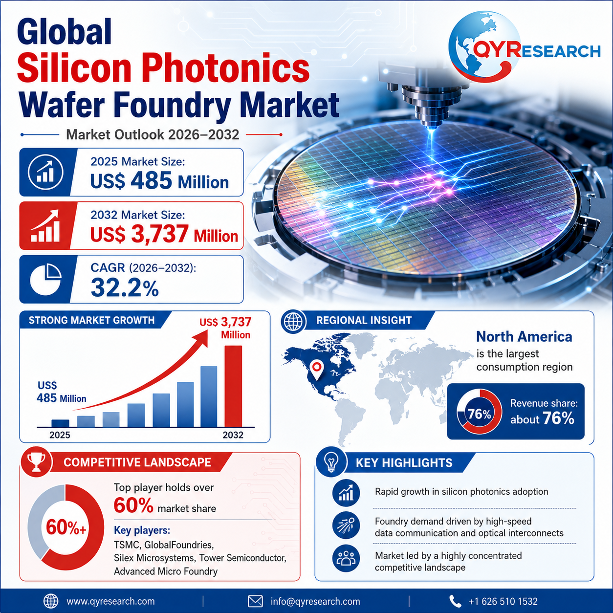
Silicon Photonics Wafer Foundry Market Analysis 2026
Global Silicon Photonics Wafer Foundry Market Size to Grow from US$485 Million in 2025 to US$3,737 Million by 2032
PUNE, MAHARASHTRA, INDIA, August 5, 2026 /EINPresswire.com/ -- Pune, India, August 5, 2026 — The global Silicon Photonics Wafer Foundry Market is entering a decisive commercialization cycle as artificial intelligence infrastructure, cloud computing, high-speed optical networking, and photonic-electronic integration create new demand for scalable wafer fabrication. A newly released industry outlook estimates that the market, valued at approximately US$485 million in 2025, could reach US$3.737 billion by 2032, representing a compound annual growth rate of 32.2% during 2026–2032.The forecast highlights a market moving beyond laboratory validation and limited pilot activity toward repeatable commercial production. In 2025, global shipments were estimated at approximately 63.73 thousand equivalent eight-inch wafers, with an average ex-factory value of about US$7,620 per wafer. For investors, researchers, semiconductor manufacturers, fabless photonics companies, optical transceiver vendors, and data center technology providers, the 2026–2032 period is expected to be shaped by process maturity, customer qualification, packaging compatibility, design ecosystem depth, and the ability of foundries to deliver stable optical performance at commercial yields.
Download Exclusive Research Report PDF Sample: (Including Full TOC, List of Tables & Figures, Chart) @ https://www.qyresearch.in/request-sample/electronics-semiconductor-global-silicon-photonics-wafer-foundry-market-insights-industry-share-sales-projections-and-demand-outlook-2026-2032
Market Overview:
Silicon photonics wafer foundry services combine semiconductor wafer manufacturing with the fabrication of photonic integrated circuits. These services typically include process design kit support, multi-project wafer shuttle runs, dedicated engineering runs, prototyping, low-volume manufacturing, and volume production. Foundries manufacture optical waveguides, couplers, modulators, photodetectors, splitters, ring resonators, thermal tuners, and related photonic structures on silicon-based wafers.
The market scope is centered on wafer fabrication revenue rather than downstream optical modules, complete co-packaged optics systems, standalone packaging and testing, pure design services, or finished end-system sales. This distinction is important because the foundry opportunity is driven by effective commercial output capability, not simply the nominal capacity of a semiconductor fabrication plant.
Silicon photonics manufacturing requires consistent wafer-level performance while also controlling optical loss, coupling efficiency, polarization behavior, thermal drift, device uniformity, electronic-photonic co-design, and compatibility with advanced packaging and test flows. These technical requirements differentiate silicon photonics foundry services from conventional mature-node semiconductor manufacturing and create opportunities for suppliers with specialized process knowledge, validated device libraries, and strong customer-support ecosystems.
Market Key Drivers:
The strongest demand catalyst is the rapid buildout of AI data centers and high-performance computing systems. As accelerator clusters become larger and data movement becomes more power intensive, conventional electrical interconnects face increasing challenges involving reach, bandwidth density, latency, and energy consumption. Silicon photonics offers a pathway to transmit greater volumes of data through optical links while supporting denser connectivity architectures.
Demand is also expanding through the transition from 400G and 800G optical modules toward higher-speed generations, including 1.6T-class connectivity and future optical input-output architectures. Pluggable transceivers remain an important near-term volume opportunity, while co-packaged optics, on-board optics, optical circuit switching, scale-up networks, and scale-out networks represent longer-term growth pathways.
The need to bring optical engines closer to switching and computing silicon is increasing the strategic value of foundries that can coordinate photonic fabrication, electronic integration, packaging, testing, and design enablement. Customers are increasingly evaluating not only the optical performance of individual devices but also the manufacturability of complete photonic architectures.
A second driver is the broadening application base. Although data center optical interconnects are expected to remain the largest growth area, silicon photonics platforms are also supporting telecom systems, coherent communications, LiDAR, industrial sensing, biosensing, medical diagnostics, quantum photonics, spectroscopy, defense research, and government-funded technology programs.
These non-data-center projects are often lower in volume and more customized, but they can generate high technical value and help foundries diversify platform utilization. Specialty applications can also encourage the development of new materials, wavelength ranges, detector technologies, low-loss waveguides, integrated light sources, and application-specific packaging methods.
Regional Insights:
North America is expected to remain a major center of commercial silicon photonics demand and production, supported by hyperscale cloud investment, AI infrastructure development, fabless semiconductor innovation, optical networking suppliers, and established foundry capability. The region’s competitive position is strengthened by manufacturing platforms that target high-volume photonics, advanced packaging, wafer-level testing, and close integration with data center customers.
The presence of cloud service providers, accelerator developers, networking equipment manufacturers, optical component companies, and semiconductor design businesses creates a concentrated customer ecosystem. This concentration may help qualified foundry platforms move more rapidly from engineering runs to commercial production programs.
Europe is likely to preserve a critical role in research, prototyping, specialty photonics, silicon nitride platforms, multi-project wafer access, and pilot manufacturing. European institutions and commercial platforms provide important pathways for universities, startups, quantum technology developers, sensing companies, and communications specialists to validate designs before moving into larger production programs.
The region’s strength in process innovation, research collaboration, specialty materials, and open photonics ecosystems should remain strategically important even as higher-volume manufacturing expands elsewhere. European organizations may also benefit from regional semiconductor initiatives intended to strengthen technology sovereignty and domestic manufacturing capability.
Asia is positioned for the fastest capacity and ecosystem expansion. Taiwan and Korea are accelerating 300 mm silicon photonics roadmaps, foundry integration, and advanced packaging strategies, while China continues to invest in domestic optical communications, data center infrastructure, and photonic supply chains.
The movement of large semiconductor foundries into silicon photonics is expected to intensify competition, improve manufacturing scale, and encourage closer alignment between photonic wafers, electronic dies, packaging platforms, and end-system qualification. Asia’s established semiconductor manufacturing base may provide important advantages in equipment access, wafer processing, outsourced assembly, testing, and supply chain coordination.
Trade policy and supply chain uncertainty will remain influential. Tariff changes, export controls, regional industrial incentives, equipment access, specialty material availability, and cross-border technology partnerships can affect costs and customer sourcing decisions. As a result, customers may increasingly evaluate dual-region manufacturing, supply continuity, intellectual property protection, and qualified second-source options when selecting foundry partners.
Market Segmentation:
By wafer type, the market is divided into 300 mm wafers, 200 mm wafers, and other formats. The 200 mm segment remains important for established platforms, multi-project wafer programs, specialty processes, and cost-conscious development. Many photonic designs have been optimized around mature 200 mm process flows, making this format relevant for both prototyping and selected commercial programs.
The 300 mm segment is expected to gain strategic importance because it offers a route toward higher manufacturing scale, greater automation, improved wafer utilization, and closer alignment with advanced semiconductor infrastructure. The format may become particularly important for high-volume AI, cloud, optical transceiver, and co-packaged optics programs that require repeatable output and integration with electronic dies.
By process platform, the market includes silicon-on-insulator and other silicon-based photonics, silicon nitride photonics, and heterogeneous or alternative silicon-based integration. SOI platforms are widely used for optical communications because they support compact waveguides, modulators, detectors, and dense photonic circuits.
Silicon nitride platforms are valued for low-loss routing, broad wavelength performance, sensing, quantum applications, and specialized communications. Heterogeneous integration is becoming increasingly important because it can combine silicon photonics with lasers, amplifiers, advanced modulators, electronic integrated circuits, and other materials that improve system performance.
By end user, demand comes from optical communication and transceiver vendors, AI and cloud data center customers, fabless silicon photonics companies, research institutes, government programs, and other technology developers. By application, the market is divided into data center and non-data-center uses.
Data centers are expected to command the largest share of incremental demand through 2032, while non-data-center applications will support platform differentiation and higher-value specialty programs. Foundries capable of serving both categories may achieve stronger platform utilization and reduced dependence on a single demand cycle.
Competitive Landscape:
The competitive field includes GlobalFoundries, Tower Semiconductor, TSMC, Silex Microsystems, VTT, SilTerra, IHP Microelectronics, imec, LioniX International, Samsung, and UMC. The market is not defined by wafer capacity alone. Competitive advantage depends on qualified device libraries, process design kit maturity, optical performance, yield consistency, turnaround time, engineering support, multi-project wafer availability, packaging partnerships, test capability, and a credible path from prototype to volume production.
GlobalFoundries and Tower Semiconductor are among the most visible commercial foundry platforms, while imec, VTT, IHP, LioniX, SilTerra, and other specialty providers contribute through prototyping, pilot manufacturing, research access, and differentiated process technologies.
TSMC, Samsung, and UMC are broadening the competitive landscape by connecting silicon photonics development with large-scale wafer manufacturing and advanced integration capabilities. This shift is likely to raise customer expectations for design portability, manufacturing reliability, packaging readiness, intellectual property protection, and global supply support.
Competition may increasingly occur at the ecosystem level. Foundries that establish relationships with electronic design automation companies, laser suppliers, packaging specialists, fiber-attachment providers, test-equipment companies, and optical module manufacturers may be better positioned to reduce customer development time and support faster qualification.
Market Trends and Dynamics:
The most important trend is the transition from standalone photonic chips toward integrated optical engines. Customers increasingly want foundry solutions that consider the complete path from design rules and device libraries to fiber coupling, laser integration, electronic interfaces, thermal management, packaging, and production testing. This favors providers with coordinated ecosystems rather than isolated process offerings.
Another major trend is the growing importance of 300 mm platforms. As demand moves from research projects to higher-volume optical connectivity, larger wafer formats can support scale, automation, and closer alignment with advanced semiconductor manufacturing. However, 200 mm platforms will remain relevant because many specialty processes, mature device libraries, and existing customer programs are already established on that format.
The industry is also moving toward more standardized design and manufacturing flows. Improved photonic process design kits, electronic design automation tools, multi-project wafer schedules, reference designs, packaging interfaces, and test methodologies can shorten development cycles and lower barriers for new entrants.
At the same time, foundries will continue to differentiate through optical loss, modulation efficiency, detector bandwidth, integrated laser options, coupling structures, thermal stability, wafer-level test capability, and overall manufacturability. Pricing will remain important, but customers are likely to place greater value on predictable yield, qualification support, secure capacity, and production continuity.
For investors, the central opportunity is the possibility that silicon photonics foundry services become a high-growth manufacturing category within the broader semiconductor ecosystem. For manufacturers, success will depend on converting technology leadership into qualified, repeatable output. For researchers and fabless companies, access to reliable process platforms and scalable production pathways will determine how quickly innovations move from experimental devices to commercial products.
Key Questions Addressed:
(1) Which wafer formats will scale fastest?
(2) How quickly will 300 mm platforms achieve qualified production?
(3) Will co-packaged optics materially accelerate foundry utilization?
(4) Which regions can establish resilient photonics supply chains?
(5) Why are AI, cloud, and data center customers becoming the most important demand group?
(6) What challenges exist around optical loss, coupling efficiency, yield, packaging, testing, and customer qualification?
(7) What opportunities exist for silicon photonics wafer foundries, fabless IC companies, optical communication vendors, data center customers, investors, and new entrants?
(8) Which companies are active in the global competitive landscape?
The 2026–2032 outlook therefore points to a market with substantial upside, but also significant execution requirements. Companies that combine process maturity, customer support, advanced integration, supply chain resilience, and volume manufacturing discipline are likely to capture the strongest opportunities as optical connectivity becomes essential to the next generation of AI, cloud, communications, sensing, and computing systems.
For Further insights and Detailed Reports, Visit: https://www.qyresearch.in/report-details/2807954/Global-Silicon-Photonics-Wafer-Foundry-Market-Insights
About QYResearch
QYResearch is a global market research and consulting company providing detailed industry analysis, market forecasts, competitive intelligence, company ranking analysis, and customized research solutions. The company supports investors, researchers, Caprylyl Glycol manufacturers, cosmetic ingredient suppliers, personal care brands, formulation developers, OEM/ODM manufacturers, raw material distributors, bio-based ingredient producers, fine chemical companies, and business decision-makers across personal care, cosmetics, chemicals, consumer goods, sustainability, healthcare, and emerging markets.
Contact US
Ankit Jain - Director, Global Digital Marketing
QY Research, INC.
India Office -
315Work Avenue, Raheja Woods, Kalyani Nagar,
Pune, Maharashtra 411006, India
Web – https://www.qyresearch.in
Email- ankit@qyresearch.com
Ankit Jain
QY Research India
+91 81497 36330
ankit@qyresearch.com
Legal Disclaimer:
EIN Presswire provides this news content "as is" without warranty of any kind. We do not accept any responsibility or liability for the accuracy, content, images, videos, licenses, completeness, legality, or reliability of the information contained in this article. If you have any complaints or copyright issues related to this article, kindly contact the author above.
